We warmly invite you to visit our laboratories.
We encourage you to familiarize yourself with the thematic offer.
To arrange a laboratory tour, please contact Ms. Anna Drzazga, who runs the campaign secretariat, tel. 22 843 68 61, e-mail:
MBE (Molecular-beam epitaxy) - how are thin layers formed?
Mgr Piotr Dziawa for groups of up to 6 people, duration approx. 30-60 min (to be agreed with the instructor), high school and 7-8th grade elementary school groups. During the laboratory tour, students will learn about the MBE technique. They will learn about the preparation for growing a thin semiconductor layer and what needs to be done to ensure that the grown material is as pure as possible.
Images obtained in a Scanning Electron Microscope (SEM)
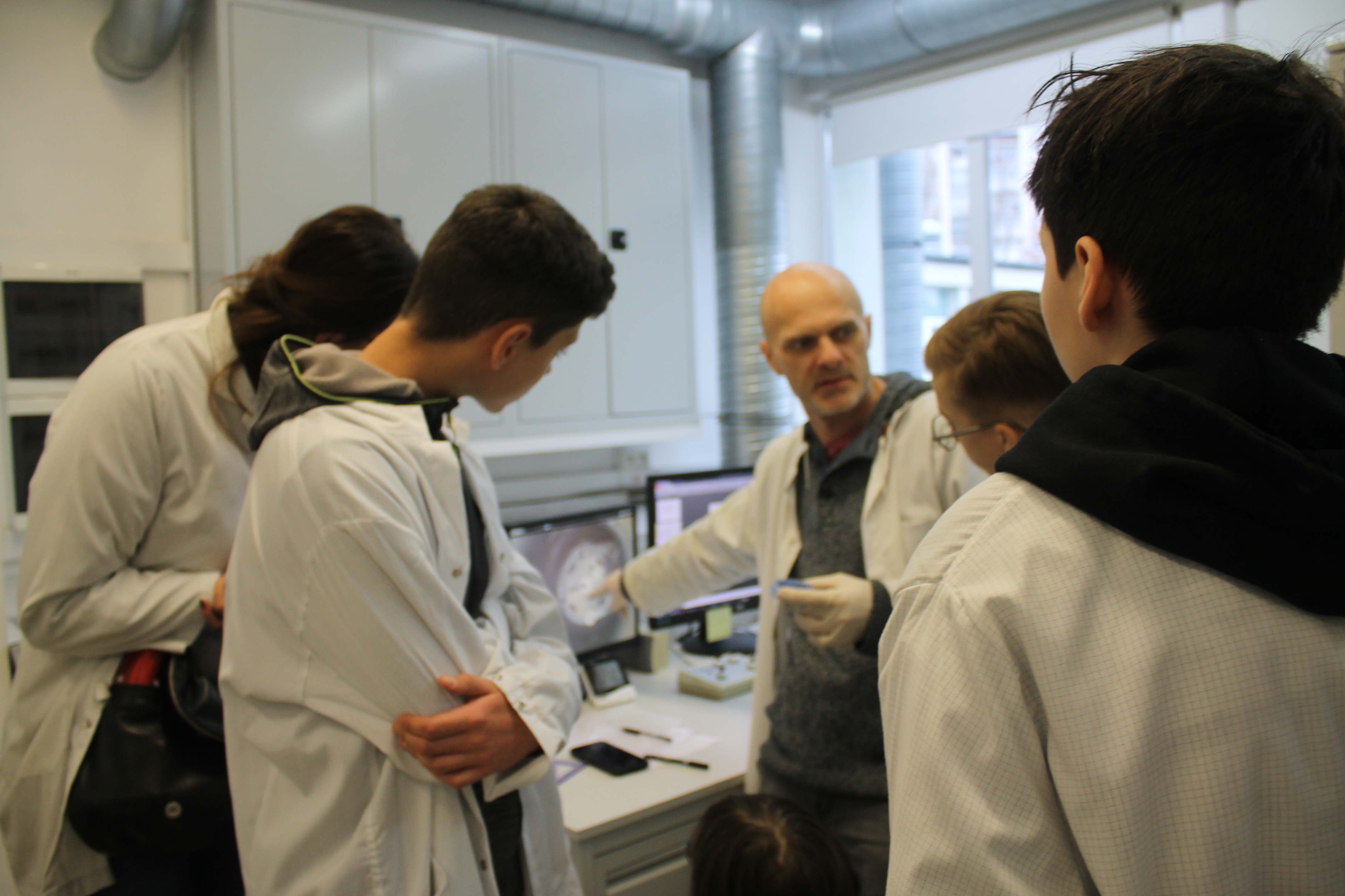
Mgr. Eng. Wojciech Wołkanowicz for groups of up to 6 people, duration approx. 30-60 min (to be agreed with the instructor), 7-8th grade elementary school and high school groups. Scanning Electron Microscope (SEM) is a basic research tool that allows for discovering and studying new and imaging existing materials, especially those invisible to the naked eye. During the laboratory tour, the structure and operating principles of the SEM microscope will be explained. The methods of interpreting images obtained in this microscope will also be discussed. The Hitachi FlexSEM 1000 scanning electron microscope used in this laboratory, with electrons accelerating voltage up to 20 kV, allows for viewing conducting materials with a resolution of up to 4nm. This microscope not only allows for viewing the sample material in very high magnification but also allows for preliminary determination of the chemical composition of the tested material. During the presentation, students will be able to observe under the microscope and learn the chemical composition of a very familiar object.
The world seen in a scanning electron microscope
Dr. Tomasz Wojciechowski - for groups of 10, lecture duration - about 60 minutes, only for high school groups. The hero of the lesson will be the scanning electron microscope. Its construction and principle of operation will be explained. Methods of sample preparation and image interpretation obtained in the microscope will be discussed. The scanning electron microscope is a fundamental research tool that allows for the discovery and investigation of new and existing materials, especially those invisible to the naked eye - materials of nanometric sizes. We have a ZEISS NEON 40 scanning electron microscope with an accelerating voltage of 0.5-30 kV and a resolution of 1.5 nm. This is a new generation microscope, completely computerized, with an electron beam lithography system from Raith. Original results from recent electron microscopy research, including electronics and materials science, will be presented. As part of the lesson, students will tour the electron microscopy laboratory.
Three-dimensional landscape of Scanning Probe Microscopy
Dr. Marta Aleszkiewicz - for groups of 10, lecture duration - about 60 minutes, only for high school groups. After scanning tunneling microscope (STM) was invented in 1981 many other microscopy techniques have been developed based upon it. So called Scanning probe microscopy uses a physical probe that scans the specimen while a quantity characteristic for the tip-surface interaction is detected. During the workshop working principles of these microscopes will be shown; we'll see the microscope "in action" and some examples of what information of the surface properties can be gained from SPM.Nanotechnology at Home - Growing Nanorods with an Induction Cooktop
Dr. Bartłomiej Witkowski, MSc Monika Ożga - for groups of up to 4 people - approx. 2-3 hours, only high school groups. Nanotechnology is a science that deals with the production and study of properties of nanostructures, i.e., objects for which at least one dimension is smaller than a micrometer. Such structures can have completely different properties and can be applied in many areas of life (detectors, sensors, automotive, electronics, medicine, etc.). The production of nanostructures is often associated with very expensive technologies, while it is possible to produce some nanostructures in a very simple and fast way. During the exercise, students will produce zinc oxide nanorods using a regular induction cooktop, and in the second part of the exercise, they will see the results of their work using a scanning electron microscope.
| © 2022 IF PAN. Realizacja* Sensorama |